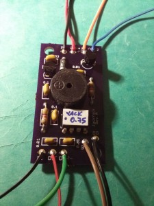
Back in October, I mentioned an open source keyer developed for the ATTINY 45 and requiring only a few components. The source code for the controller and an example schematic were uploaded to a repository. Subsequently, I decided to try my hand at producing a PC board. Rather than try some sort of printer-based method based on toner transfer, I wanted to try going a more professional route and having the PCB run off by a fab. Initially, I thought I’d have to go overseas and wait upwards of a month for my boards to come back, but I found a domestic fab that provides an amazing service for low volume prototype boards: OSH Park.
I had already laid the schematic out in Eagle CAD, which seems to be popular among hobbyists. Most of my components were available in off-the-shelf libraries, but I had to layout the piezo speaker as a custom part (although I started from another similar piezo speaker and just had to modify the dimensions). It took a while to get the hang of laying everything out on the PCB, laying down ground planes, routing the traces, and making the silk screen look nice, but after many hours with online tutorials, it all looked right. I ran some rules checks, and everything reasonable, as far as I could tell.
Next, I shopped around using the online check and quote tools available from a number of popular fab houses. To upload my design, in most cases, I had to send a zip file of the various Gerber layers — top copper, bottom copper, top silk, etc. But, for OSH Park, all I had to do was upload the Eagle board file itself. This makes a lot of sense, as the Gerbers are generated from that file, so all the information is already there in the board file.
The OSH Park site interprets the board file on the fly and provides a rendering of approximately what the board will look like when final. There are a number of options regarding cost, turn around, etc., but I opted to get three copies of my design for about ten dollars by agreeing to have my boards made as part of a larger run to take place in about two weeks from the date of submission. The way OSH Park makes prototype boards affordable is by merging multiple designs into one larger board and then cutting that board apart. Their cost is per square inch, and I had designed my board to be one by two inches — not bad considering that I used all through-hole components and did not go out of my way to pack them tight on the surface of the board. In fact, my design is a little generous in that I give a number of ground connection points, whereas only one is really necessary for the sake of wiring in external components.

From the time of submission until the envelope arrived, I was able to track progress of the order, so there was particular excitement on the day that I knew the package would be waiting in my mailbox. When I opened the padded shipping packet up, I found three little purple boards, just about identical to the rendering that was provided when I had uploaded the design.
The PC boards are excellent quality, with no alignment issues. The solder mask went where it was supposed to go, all the vias are functional, and the pads take solder well and have no tendency towards lifting. Components went onto the board without any fuss and when powered up, the board worked perfectly, the first time. Having verified that the design works, I’ve shared the board on the OSH Park website.
Now that this seems to be working, one option would be to run off more copies of the boards and do something with them — embedded keyers, stand alone kits, etc., but now that I’ve tried out designing a through hole board, I’m curious how much more compact the design would be with surface mount parts (and how much more difficult it would be to assemble).


I’m not finding a schematic.
Have I not looked in the correct places?
Good point — GoogleCode has went belly up a while back — everything has moved over to github:
https://github.com/dhakajack/jackyack
73,
Jack
5R8SV / AI4SV
I finally got around to building up one of you boards. My “shack” version was built on protoboard. The board quality is great!
For a stand-alone keyer, the voltage regulator seems to be less practical than battery power, as the 78L05 regulator itself draws as much power as does the ATTINY85. The ATTINY85 powers down into ultra low-power mode after 60 seconds regardless of power source. It’s easy enough to simply solder a CR2032 battery holder + lead to the power side of the reset resistor and bypass the regulator. The regulator would be nice if installed inside a rig.
Brief video of my build (running my customized version of your code changes) at:
https://www.youtube.com/watch?v=odJTkdFPuio
Best,
Don
Amazing piece of art with many options and clever software solutions in a 8Kbytes of program. Works like a charm. Brilliant. Thanks a lot.
73s,
Sergio/W4CVV
Hello Jack
Everything good but the speed on my two programed ATtiny 85 v.075. After tip a “U” on the command mode it’s give to me poor 4s run instead 20s. The out speed is appx 5x more. I programmed on avrdude using “make program” with USBasp programmer.
Any good advice is welcome.
73 de Davor, 9a4kj